Flip chip technology
Flip chip technology was invented by IBM in 1960’s. Originally the technology was knows as Controlled Collapsed Chip Connection (C4) but later the technology and its variations have been know just as flip chip. In flip chip process, IC wafers are metallised and electrically conductive bonding medium is deposited at the terminal pads., wafers are diced to chips and the chips are bonded face-to-face with another chip or printed circuit board. The typical IC wafers have aluminum of copper metal finishing at the terminal pads and these metal layers cannot not soldered as they are in reliable way. The pads have to be at least metallised with noble metals to restrict oxidation (Au, Pt, Pd, Ag etc.) and diffusion effects a(Ni, Cu, Pt, etc.) the bonding interface and hence enable stable bonds. In the typical flip chip processes the terminal pads located at the perihery of the chips are redistributed in area-array format on top of polymer dielectric layer. In flip chip of hybrid pixel detectors the redistribution process won’t be necessary because the pixels are already segmented in area-array format.
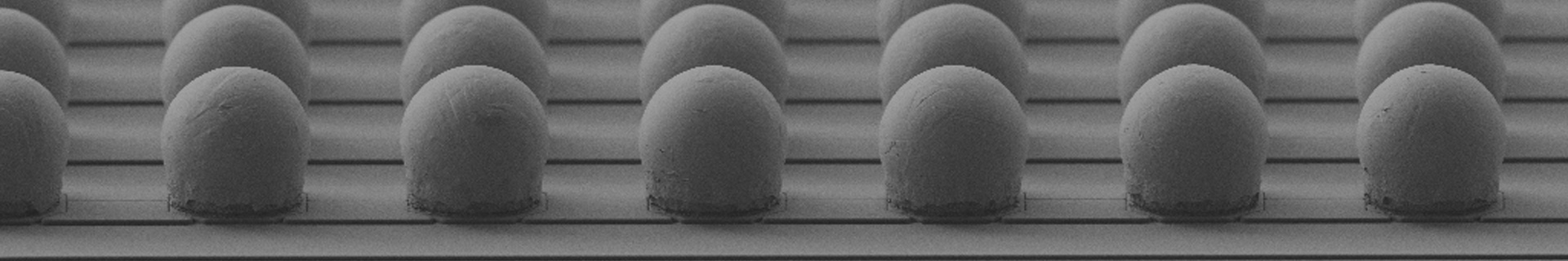
Flip chip bonding is an ideal interconnect technology for hybdrid pixel detetors (i.e., joining a large matrix of pixels together in a repeatable and controlled manner). This is because the connections are within the footprint of the chip and the interconnects don’t take up any additional space, maximizing the sensors active area. In flip chip bonding solder bumps or conductive adhesives are needed to make the electrical-mechanical interconnections between the chips. Typically a solder bump is grown on each pixel on the readout chip and sensor chips have solderable Under-Bump Metallisation (UBM). As there is a solder bump interconnection for every pixel, the bumping quality and flip chip yields have to be very high to avoid visible defects in the radiation image. As the sensor and readout chips are relatively large and the number of bump connections is high (1,000-100,000) the flip chip yield of hybrid pixel detectors is typically determined by the success rate of the bumping process.
Cross-section of hybrid pixel detector; sketch and SEM image
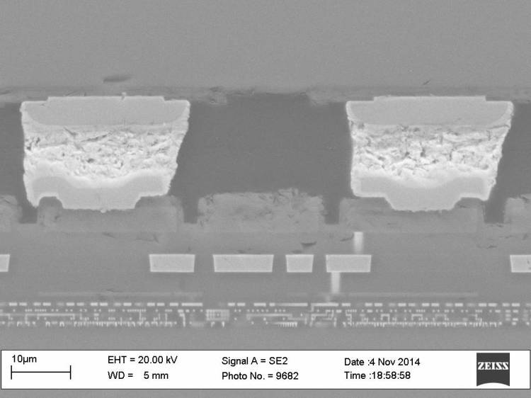
SEM image; CMOS ASIC at bottom
Solder bump and Under-Bump Metallization deposition on wafers
Everything under this paragraph is considered from hybrid pixel detecor point of view (large chips and fine pitch). In typical flip chip processes solder bumps, adhesives, indium or gold studs are used. Each of these have their strenghts and weaknesses and different challenges in the deposition process.
Electroplating has been widely used in deposition of flip chip bumps because rather high deposit rate, well understood chemistry and good deposition uniformity. Moreover, both the UBM and the solder bump will be deposited in sequence using the same potoresist mask. Bump deposition based on electroplating is rather cost-intensive because it requires Physical Vapor Deposition (PVD) and lithography processes. Electroplating process requires typically one mask layer and one lithography round. UBM/solder is deposited galvanically at the photoresist openings and after the removal of the photoresist, the deposited metal layers act as a mask for etching the conductive seed layers from the wafers. Despite the simplicity of the electroplating, the process is very sensitive for chemical compatibility of different materials.
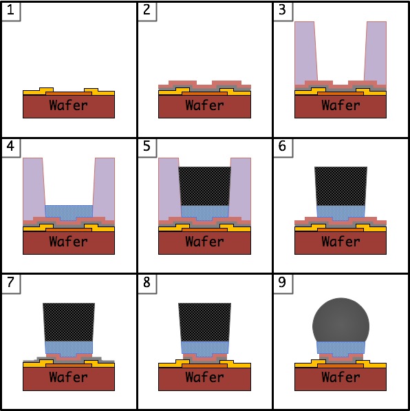
Picture depicts one pixel in different steps of electroplating process: 1) cleaning of wafers, 2) field metal deposition (adhesion/seed layer), 3) thick photoresist lithography, 4) electroplating of UBM, 5) electroplating of solder, 6) stripping of photoresist, 7) wet etching of seed layer, 8) wet etching of adhesion layer & 9) solder reflow.
Evaporation combined with lift-off processing is an alternative way to deposit the UBM and the solder/metal material at the bonding pads. The down side is the very slow deposition rate and the complexity of the thick photoresist lift-off process. The bright side of evaporation is the uniformity is very good and easy deposition of different metals and alloys. Indium bumping is the perhaps the best example of using lift-off process within hybrid pixel detectors. Indium is deposited on both sides of the chips to be bonded and it enables thermocompression bonding at lower temperatures than the melting point of indium. Perhaps, the greatest strenght of the lift-off process that it is compatiple with ultra fine pitch flip chip interconnects and it can beat electroplating in terms of bumping resolution.
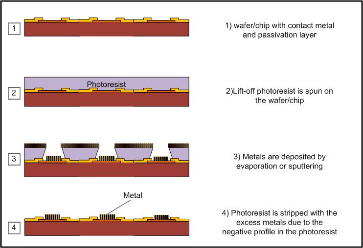
How lift-off works
Micro-packaging of electronics is a cost driver in case of most of the microelectronics devices.and thus low-cost technologies have been developed. During the last 20 years, alternative bumping/ UBM desposition technologies have been emerging such as Electroless Nickel – Immersion Gold (ENIG) which can be used in a combination with adhesive bonding and solder ball placement. In many cases the ”low cost” alternatives mean that the lithography process can be avoided and that reduces the amount capital cost required for setting up a flip chip line. ENIG metal finishing comprises of a chemically grown Ni layer (> 3 um) on top of Al or Cu metallisation and a thin gold layer (~50 nm) which protects Ni from oxidation. ENIG UBM is solderable and glueable and can also be used with Anisotropic Conductive adhesive Films (ACF).
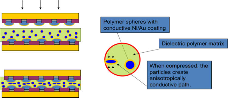
ACF with conductive particles is compressed between elevated UBM pads and electrical interconnects are formed at those places.
Novel ways to deposit solder or adhesive on top of an UBM pad are solder ball jetting, and ink jet printing. Dispensing of adhesives is also possible through a nozzle by droplet formation, but the pitch is limited to 150-200 um. In solder ball jetting, the preformed solder balls with any solder material and diameter of 30-100 um can be shot on the UBM pads in molten state. The technology goes very well together with the ENIG UBM technology. The preformed solder balls are very uniform in size and they even can be even transferred on wafer on one step by using wafer-level gripping mechnisms. By using state-of the-art inkjetting one can very precisely make ”bumps” by piling tiny droplets of conductive ink or adhesive. Both solder ball placement and inkjetting might be viable solutions for bumping of compound semiconductor sensors.
Summary: As there are many different ways of doing the wafer bumping, it is important to point out that the different methods might require different design rules and different UBM pads. Before fabricating wafers and having them flip chip processed at some packaging foundry, it is worthile to check the design rules with the foundry to avoid disappointments in future.
Flip chip bonding
In flip chip bonding (AKA bump bonding) the readout and sensor chips are mated face-to-face using solder bump, adhesive bump/film or metal bonds. If the bumps have good height unifomity, it is very likely that the bonding will also succeed. Because pixel sensors have typically a high number of small bumps, it is necessary that the bumps will be equally compressed accross the chips to be bonded to avoid either solder pridges or open flip chip joints. It is very useful to have ”levelling feature” incorporated in the bonding equipment. The levelling can be done by optical autocollimator, laser or by smart mechanical solutons that can spread the bonding force uniformly over the chips.
Flip chip bonding of silicon hybrid pixel sensors is relatively simple with fairy fine pitches (>100um) but as the pitch gets smaller and the number of bumps increases it becomes more challenging. The smaller the picth, the more uniform the solder bumps required. When going down for 30 um pitches or smaller, the mechanical force required for bonding becomes very high and not many of the equipment can be used anymore.
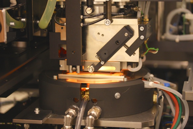
Flip chip bonder in operation
Bonding of the pixel detectors differs from the mainstream flip chip bonding in the sense that commercial (small) IC chips are placed on reels and the bonding system feeds the chips and bonds them in seconds. In addition the size of the bumps is significantly larger than on the pixel chips. The large and very sensitive sensor chips cannot be placed on reel and they require manual handling. Also the very fine pitches require very robust and stable bonding equipment and that effectively slows down the bonding rate.
Flip chip bonding of compound semiconductor detectors is much more demanding than just silicon chips. With silicon chips the Coefficient of Thermal Expansion (CTE) is very similar for the silcion used for the sensor and the readout chip. In this respect, almost any kind of solder alloy with a melting point below 400 C can be used for bonding Si pixel detectors. When bonding compound semiconductors such as CdTe, CdZnTe (CZT) or GaAs, the CTE will be different from that of Si which will limit the available solder alloys. In other words, the CTE mismatch favours using low melting point solder alloys. Moreover, CdTe and CZT have temperature limitation because of the degredation of the sensor material at elevated temperatures and thus bonding temperatures below 150C are desirable. There are not many widely available solder allouys that can meet this criteria and the most commonly used binary solder alloys are BiSn (MP 138C) and InSn (118 C). With compund semicondutor sensors it is beneficial to use little larger solder bumps than with Si sensors because the higher joints will adapt to the shear stresses caused by the CTE mismatch better.
Compound semiconductor sensor used for CT imaging have typically large pitch (> 200 um) and thus it is better to use adhesive bonding than solder bonding because there are many adhesives that can be cured close to 100 C. From flip chip point of view the quality of the compound semiconductor sensor chips depends on the quality of pixel metallisation and also on the planarity. The pixel metallisation has to be solderable and the chips have to polished so that the cathode side won’t be convex and the pixel side is planar.
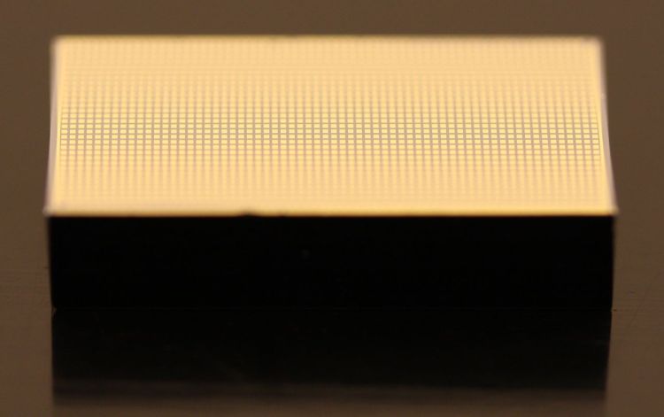
Compound semiconductor sensors might differ significantly from silicon sensors. For example, a 5 mm thick CZT sensor in the picture.