Sensor Technology
Since the radiation is converted into electric charge directly the sensor materials used on devices described here are called “direct converting”. They are typically based on silicon, CdTe, CdZnTe or GaAs semiconductors and semi-insulators. Materials such as Ge and diamond has been utilised as well. Silicon is the most commonly used material due to its uniformity, lack of defects and mature process technology.
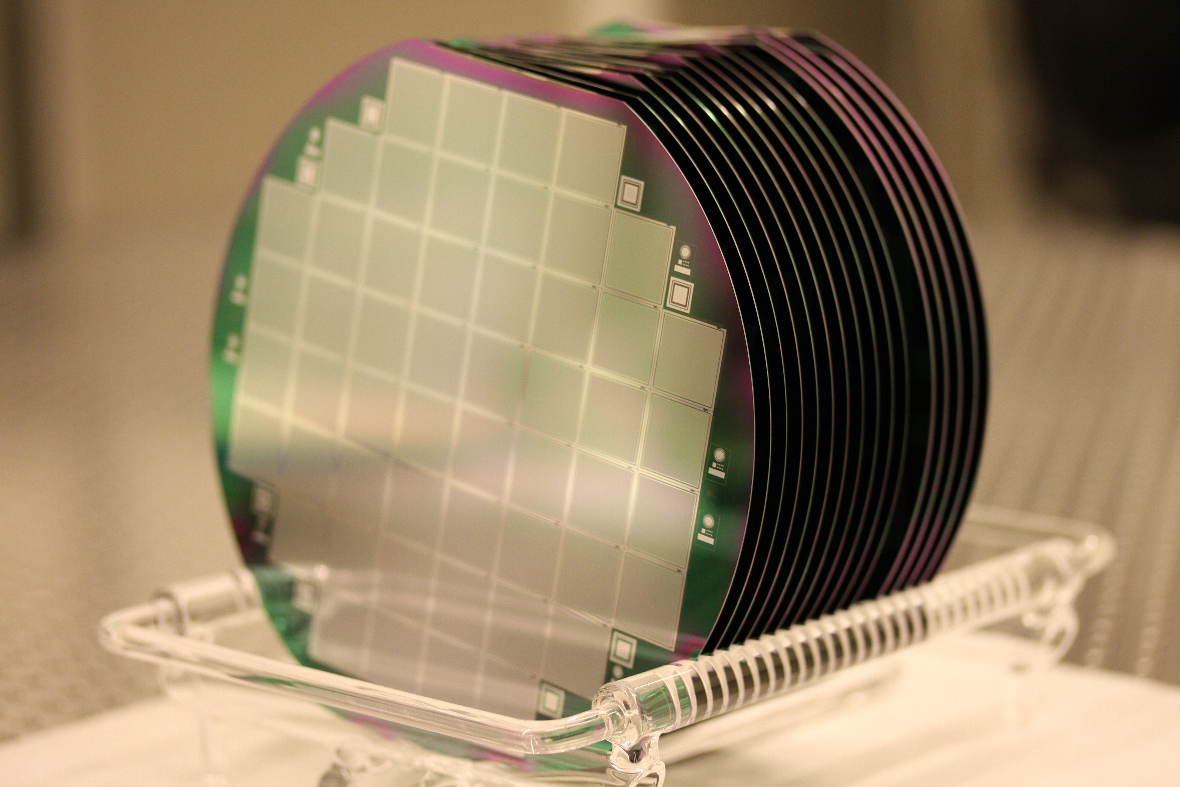
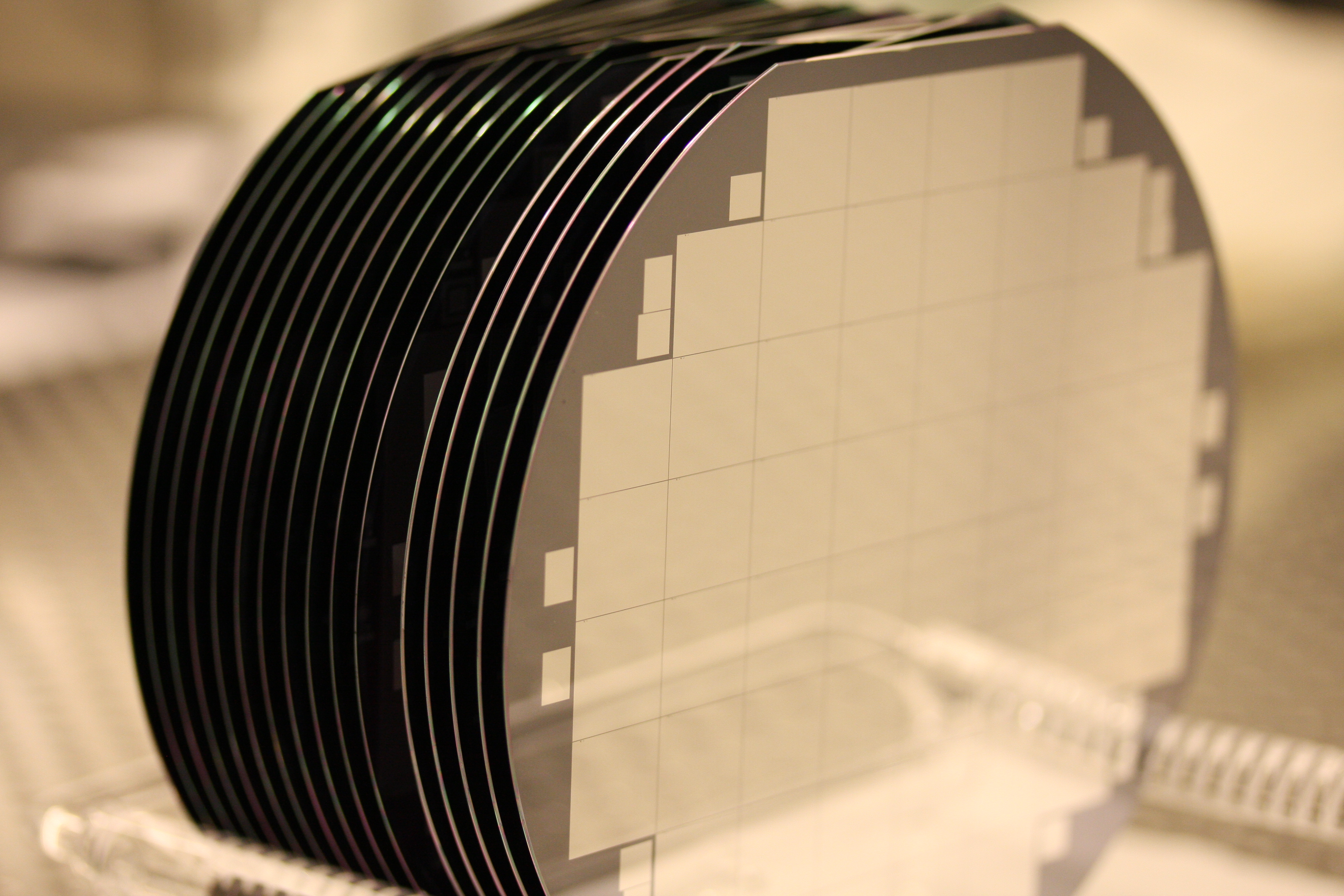
Silicon sensor process technology allows pixel sensors with various pixel pitches down to 25 um. The sensors are typically manufactured on wafers with diameter of 4″ (100 mm) or 6″ (150 mm). Standard silicon sensor processing allows planar pixel sensors with thicknesses from 300 μm to more than 1 mm thickness. To manufacture thinner sensors requires special process steps and clean room tools.
-
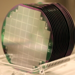
- Pixel side of planar silicon sensors on 6″ wafers of various thicknesses.
-
- Cathode side of planar silicon sensors on 6″ wafers of various thicknesses.
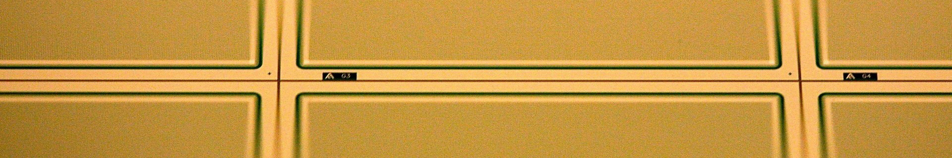
-
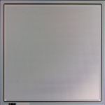
- Planar Si pixel sensor.
Planar Si pixel sensor
The planar “standard” silicon sensor has a guard ring structure surrounding the active pixel matrix. It is used to draw the excess leakage current from the sensors’s dicing damage and to allow higher breakdown voltage. Typically single grounded guard ring is accompanied with one to several floating guard rings depending on the reverse bias voltage tolerance requirements. Width of the guard ring structure is from 500 μm to 1 mm. The sensor volume below the guard ring structure is insensitive to the absorbed radiation, i.e. the charge of the radiation is not collected by the active pixel matrix and its information content is lost.
Area of the planar sensors can range from 1 cm² to few 10 cm² thus allowing single or multiple readout ASICs for integration. Industry is providing planar technology products with a single ASIC modules, quad (4) ASIC modules, hexa (6) modules up to 16 ASIC modules.
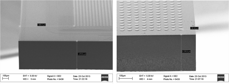
Planar Si pixel sensor with guard ring structures that cause almost 1 mm insensitive volume outside the active pixel matrix (left). Edgeless Si pixel sensor, which has fully sensitive detection volume (right). In both images the pixel pitch is 55 um.
Edgeless Si pixel sensor
The edgeless (active edge) sensor doesn’t have guard ring structure surrounding the active pixel matrix and thus tiling of the edgeless pixel sensors can cover large areas without insensitive areas in the field of view. The sidewalls of edgeless sensors are “activated”, which means that the depleted volume of the sensor can completely cover the physical volume of the sensor and thus it lacks the insensitive volume that is characteristic of the planar pixel sensors. The edges can be “activated” by creating a conductive or resistive edges. The conductive edge activation extends the cathode doping and bias potential to the sidewall edges. It causes the electric field lines of each pixel to bend close to the activated edge. In case of resistive edge the bias potential is dropped along the depth of the activated edge and less bending of the electric field lines is observed.
The edgeless Si sensor process technology is much more complicated then the planar sensor processing since it requires a temporary wafer bonding of the handle wafer and advanced lithography. Nevertheless the handle wafer technology allows feasible realisation of variety of pixel sensor thicknesses from few micrometers up to 700 μm. More detailed description of the edgeless sensor process technology can be found for example from an industrial provider’s website. In addition, realisation of 3D pixel sensor structures doesn’t add too much the process complexity.
3D Si pixel sensor
The 3D electrode structure was proposed almost two decades ago by group of Prof. Sherwood Parker. The current development of the technology is mainly carried out by the ATLAS 3D sensor community. In the planar sensor technology the anode and cathode of the pixel sensor are on the front and backside of the sensor and thus the distance between the anode and the cathode is determined by the sensor thickness. Instead in the 3D pixel sensor the anode and cathode electrodes have been manufactured through the bulk of the silicon wafer and the distance between the two electrodes can be freely determined. Benefits of the technology are low operational bias voltage, small charge sharing and high radiation damage tolerance. The benefits are gained with increased process complexity. Currently there is no industrial provider for the 3D pixel sensors.
Regardless of the type, all sensors need to be attached to the readout chip. The technology applied there is called flip-chip bonding and it is explained in the next article.